BJT Transistor Simulator
NPN & PNP — Simulate · Explore · Practice · Quiz
Adjust VBE and VCE to see how the transistor operates. Press Run to animate carrier flow.
User Guide
1 Overview
The BJT Transistor Simulator visualises how bipolar junction transistors work at the semiconductor level. See electrons and holes flow through NPN and PNP structures, watch depletion regions respond to bias voltages, and observe breakdown mechanisms in real time.
Four modes: Simulate (interactive animation), Explore (educational cards), Practice (unlimited problems), and Quiz (5-question assessment).
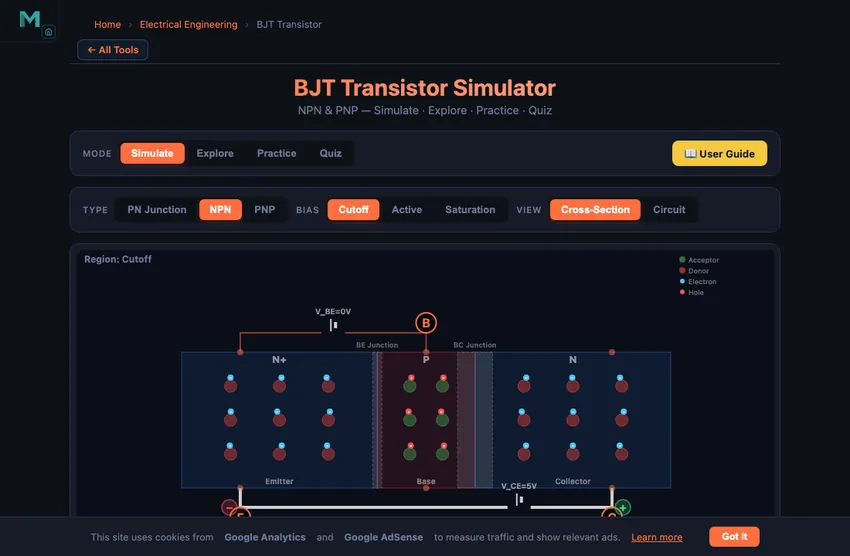
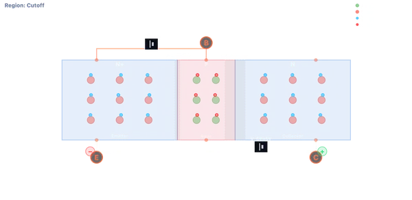
2 Building the Circuit

Choose NPN or PNP transistor type. Adjust VBE (base-emitter voltage) and VCE (collector-emitter voltage) using the sliders. Press Run to see animated carrier flow. The description panel explains what is happening physically at each bias point.
3 Energising the Circuit
The cross-section view shows the three doped semiconductor regions (Emitter, Base, Collector) with their junctions. Blue dots represent electrons, red dots represent holes. The depletion regions (grey/hatched zones) shrink or grow based on bias.
Key observations:
- Increase VBE past 0.5V to see the BE junction turn on
- At VBE ≈ 0.7V with VCE > 0.2V: Active mode — electrons flow E→B→C
- Reduce VCE below 0.2V: Saturation — both junctions forward biased
- Use the Avalanche preset to see cascade impact ionisation
- Use the Zener preset to see quantum tunnelling at the BE junction
Right-click the canvas to save as image, copy data, or reset.
4 Circuit Theory
Five educational categories: Basics (PN junctions and BJT structure), Operating Regions (cutoff, active, saturation), Breakdown (avalanche, Zener, punch-through, thermal runaway), Formulas (Ebers-Moll, I-V equations), and Applications (amplifiers, switches, biasing circuits).
5 Try a Problem
Practice: Solve problems about BJT regions, current calculations, and breakdown identification. Instant feedback with explanations.
Quiz: 5 randomly selected questions. Scored with a star rating.
6 Key Concepts
Current gain: β = IC / IB (typically 50–300)
KCL: IE = IC + IB
Active mode: IC = β × IB, VBE ≈ 0.7V
Saturation: VCE(sat) ≈ 0.2V, both junctions forward biased
Breakdown: Avalanche (>5V, impact ionisation), Zener (<5V, tunnelling)
7 Tips & Best Practices
- Use presets to jump to each operating region and observe the differences.
- Watch the depletion region width change as you sweep VBE from 0 to 0.8V.
- Compare NPN and PNP — carrier types are reversed but principles are identical.
- In Explore mode, read the Breakdown category before attempting breakdown questions.
- Audio feedback: click on interaction, success/error tones in Practice and Quiz.
Understanding BJT Transistors: NPN and PNP

What Is a BJT Transistor?
A Bipolar Junction Transistor (BJT) is a three-terminal semiconductor device that uses two PN junctions to control current flow. The three regions — Emitter, Base, and Collector — are alternately doped to form either an NPN or PNP configuration. A small current at the base terminal controls a much larger current between collector and emitter, making BJTs essential for amplification and switching.
NPN vs PNP: How They Differ
In an NPN transistor, the emitter injects electrons into the thin P-type base. Most electrons cross the base and are swept into the collector by the reverse-biased BC junction. In a PNP transistor, holes are the majority carriers — they flow from emitter through the N-type base to the collector. The physics is identical; only the carrier types and voltage polarities are reversed.
Operating Regions and Breakdown
BJTs operate in four regions: Cutoff (off, both junctions reverse biased), Active (amplification, IC = β×IB), Saturation (fully on, VCE ≈ 0.2V), and Reverse Active (rarely used). Beyond normal operation, two breakdown mechanisms are critical: avalanche breakdown (impact ionisation cascade at high VCB) and Zener breakdown (quantum tunnelling at heavily doped junctions).
The Three Amplifier Configurations — CE, CB, CC
A BJT can be wired in three fundamentally different amplifier topologies, depending on which terminal is shared between input and output.
| Config | Voltage gain | Current gain | Input impedance | Where it lives |
|---|---|---|---|---|
| Common Emitter (CE) | High (50−200×) | High (β ≈ 100) | Medium (~1 kΩ) | General-purpose amplifiers; the workhorse |
| Common Base (CB) | High | ~1 (α ≈ 0.99) | Very low (~50 Ω) | High-frequency RF amplifiers; cascode stages |
| Common Collector (CC) / Emitter Follower | ~1 (less than) | High | Very high (~100 kΩ) | Buffers; impedance matching; output drivers |
Most analogue circuits use a mix: a CE stage for voltage gain, then a CC (emitter follower) at the output to drive a low-impedance load without losing the gain you just built. CB is reserved for specific high-frequency applications where its low input impedance is an advantage.
A BJT Worked Example — Simple Common-Emitter Amplifier
Design a CE amplifier: VCC = 12 V, β = 100, want IC = 1 mA. Pick RC and find RB.
| Step | Working | Result |
|---|---|---|
| Want VCE at mid-supply | VRC = VCC/2 = 6 V | — |
| Collector resistor | RC = VRC/IC = 6/0.001 | 6 kΩ |
| Base current required | IB = IC/β = 0.001/100 | 10 µA |
| Base resistor (VBE = 0.7 V) | RB = (VCC − VBE)/IB = (12−0.7)/10×10−6 | 1.13 MΩ |
| Voltage gain (small-signal) | Av = −gmRC ≈ −(IC/VT)·RC = −(40×10−3)·6000 | −240 |
That last row is the magic: a 1 mV input swing on the base produces a 240 mV swing at the collector, inverted. With careful biasing and proper capacitor coupling, this is the basis of every audio preamp and signal-conditioning circuit since 1950.
References for BJT Analysis
- Sedra & Smith — Microelectronic Circuits, 8th ed., Chapter 6 (BJT Transistors).
- Boylestad & Nashelsky — Electronic Devices and Circuit Theory, 11th ed.
- Horowitz & Hill — The Art of Electronics, 3rd ed. Chapter 2 covers BJT amplifier design with great practical insight.
Explore Related Simulators
Continue your electronics learning with our Ohm's Law Simulator for circuit fundamentals, Capacitor Bank Simulator for energy storage and RC circuits, Ray Optics Simulator for physics exploration, or the Litmus Test Virtual Lab for chemistry.